Datasheet4U Logo Datasheet4U.com

TC7SP3067TU - Low Voltage Dual Supply Single Bus Switch

This page provides the datasheet information for the TC7SP3067TU, a member of the TC7SP3066TU Low Voltage Dual Supply Single Bus Switch family.

Features

  • Operating voltage range: VCCA = 1.1 to 2.7 V (Control portion) VCCB = 1.65 to 3.6 V (Switch portion).
  • ON-resistance: RON = 8 Ω (max) (VCCB = 2.7 V) RON = 10 Ω (max) (VCCB = 2.3 V).
  • ESD performance: Machine model ≥ ±200 V Human body model ≥ ±2000 V.
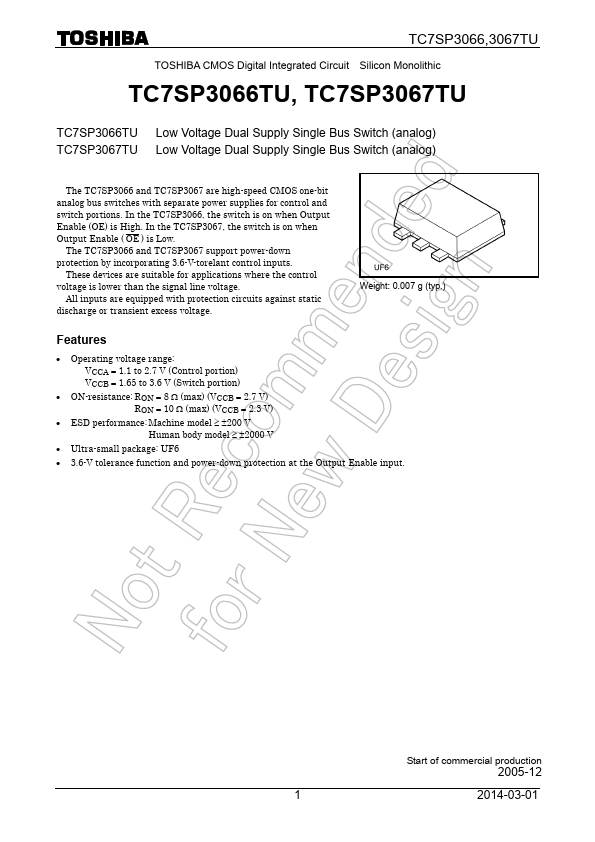
  • Ultra-small package: UF6.
  • 3.6-V tolerance function and power-down protection at the Output Enable input. Start of commercial production 2005-12 1 2014-03-01 Pin Assignment (top view) TC7SP3066TU VCCB.

📥 Download Datasheet

Datasheet preview – TC7SP3067TU

Datasheet Details

Part number TC7SP3067TU
Manufacturer Toshiba Semiconductor
File Size 212.54 KB
Description Low Voltage Dual Supply Single Bus Switch
Datasheet download datasheet TC7SP3067TU Datasheet
Additional preview pages of the TC7SP3067TU datasheet.
Other Datasheets by Toshiba Semiconductor

Full PDF Text Transcription

Click to expand full text
TC7SP3066,3067TU TOSHIBA CMOS Digital Integrated Circuit Silicon Monolithic TC7SP3066TU, TC7SP3067TU TC7SP3066TU Low Voltage Dual Supply Single Bus Switch (analog) TC7SP3067TU Low Voltage Dual Supply Single Bus Switch (analog) The TC7SP3066 and TC7SP3067 are high-speed CMOS one-bit analog bus switches with separate power supplies for control and switch portions. In the TC7SP3066, the switch is on when Output Enable (OE) is High. In the TC7SP3067, the switch is on when Output Enable ( OE ) is Low. The TC7SP3066 and TC7SP3067 support power-down protection by incorporating 3.6-V-torelant control inputs. These devices are suitable for applications where the control voltage is lower than the signal line voltage.
Published: |